Does India have what it takes to lead the Advanced Chip Packaging revolution?
/ 5 min read
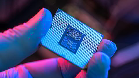
Credits: Getty Images
Does India have what it takes to lead the Advanced Chip Packaging revolution?
India is making significant strides in the semiconductor industry with government-approved chip fabrication and packaging plants. The focus on advanced packaging technologies, driven by AI and high-performance computing demands, positions India to become a global hub. Experts believe strategic partnerships and increased government incentives are crucial for India's success in this competitive field.
This summary is AI-generated, and Fortune India is not responsible for its content or any associated copyright issues.
Sources in the Ministry of Electronics & IT (MeitY) suggest that Semicon 2.0 will prioritise the advanced packaging of semiconductors or chips.
Credits: Getty Images
India’s ambitious semiconductor mission has made significant strides, with one chip fabrication unit and four testing and packaging plants already having secured government approval under its incentive scheme, launched in 2020 and revised in 2024.
Sources in the Ministry of Electronics & IT (MeitY) suggest that Semicon 2.0 will prioritise the advanced packaging of semiconductors or chips. While legacy chip packaging remains relevant, the future of semiconductors lies in advanced packaging technologies, which are crucial for enhancing performance, power efficiency, and integration in next-generation chips.
Manish Rawat, a semiconductor analyst at TechInsights, says rising demand for artificial intelligence, data centres, smartphones, and automotive electronics is driving the need for high-bandwidth, low-latency, and power-efficient chips, making advanced packaging essential.
“Advanced packaging is crucial for overcoming traditional scaling limits by enabling heterogeneous integration, combining different chip types to enhance performance and energy efficiency,” says Rawat. Advanced packaging is a cost-effective alternative to expensive advanced node fabrication, as it improves chip functionality without relying solely on complex process nodes, according to Rawat.
Reshaping the Semiconductor Industry
Traditionally, semiconductor chips were designed to execute a single function or process. But as computing demands surge—driven by AI, high-performance computing, and advanced connectivity—the need for more transistors per chip continues to grow. Advanced packaging facilitates this integration by minimising the size of electrical contacts, significantly enhancing chip performance and efficiency.
Danish Faruqui, CEO of Fab Economics, says, “Advanced Packaging has now become the focal point of both semiconductor product performance and volume supply, determining the attributable revenue. Today, all semiconductor leadership products that are the true moat of competitive advantage of end devices across every end market are made possible only by Advanced Packaging architectures,” says Faruqui. Fab Economics is a US-based consultancy serving fabricators and OSATs, and offering semiconductor investment services.
Faruqui says NVIDIA’s H100 and Blackwell GPUs, the hardware responsible for all the use cases of Generative AI/ChatGPT, require integrated compute, connectivity and storage performance by heterogeneously integrating seven very large die blocks.
Taiwan’s TSMC, the leading semiconductor foundry, makes this highly complex packaging possible by using packaging architectures such as CoWoS-S (chip on wafer on substrate–silicon interposer) or CoWoS–LSI, which is CoWoS with local silicon interconnect.
In 2019, advanced packaging accounted for 42.6% of the total semiconductor packaging market. Driven by demand for high-performance and power-efficient chips, the share of advanced packaging is increasing and is projected to reach nearly 50% by 2025.
According to Yole Development, the advanced packaging market was valued at approximately $28.8 billion in 2019. It is expected to grow at a CAGR of around 7% to $42.2 billion by 2025.
{{#most-powerful-women-snapshot-individual.slug}} {{/most-powerful-women-snapshot-individual.slug}} {{^most-powerful-women-snapshot-individual.slug}} {{/most-powerful-women-snapshot-individual.slug}} {{#showRanking}} {{current-rank}} {{/showRanking}} {{#photo.0.url}}
{{name}}
Yet only a few companies and nations dominate this space, much like the semiconductor fabrication ecosystem. Advanced packaging capabilities are heavily concentrated in regions with established semiconductor supply chains, leaving much of the world dependent on a handful of players for cutting-edge packaging solutions.
Gaurav Gupta, VP analyst at Gartner, says advanced packaging is led by foundries (TSMC/ Samsung/ Intel) and by traditional OSATs or outsourced semiconductor assembly and test units such as ASE/Amkor. These facilities are spread across Taiwan, South Korea, China, Vietnam, and Malaysia.
This concentration has occurred mainly because an ecosystem has developed, says Kanishka Chauhan, a Senior Principal Analyst at Gartner. Taiwan and Korea have abundant expertise and good infrastructure, as the foundries and testing facilities were built there. “Even the governments incentivise expenditures on research and development, fostering emerging technologies, including advanced packaging,” says Chauhan.
TSMC, Samsung, Intel, SK Hynix, Micron, ASE, Amkor, JCET, KYEC, and Power Tech are expanding their advanced packaging operations globally, according to Fab Economics Greenfield OSAT practice. The projects cover greenfield ground broken, greenfield announced and greenfield speculative projects, from 2024-2030.
The Opportunity Ahead
By securing advanced packaging projects, India could become a global semiconductor hub. A potential game-changer would be an Intel advanced test and manufacturing facility in India, which could catalyse ecosystem development. Intel can be a critical enabler for building the semiconductor ecosystem in India due to two different advantages – a mature OSAT partner and supplier ecosystem, and a roadmap to advanced packaging.
Faruqui believes these areas will enable India to leapfrog development by five to seven years individually. “Intel, being the longest-standing player in the segment, has the potential to bring on board the entire ‘mature’ ecosystem for back end in India,” Faruqui says.
The other OSAT players are entering the semiconductor business for the first time and building the partner and supplier ecosystem, he points out.
Faruqui believes Intel is ahead of TSMC and Samsung in advanced packaging technology.
Industry watchers believe the government should increase incentives for advanced chip packaging in Semicon 2.0, and also consider offering tax incentives and subsidies, such as reduced corporate tax rates and R&D credits, to lower entry costs.
Rawat says, “Infrastructure support through SEZs and technology parks with reliable utilities and logistics can create a competitive environment. R&D support and collaboration via public–private partnerships can drive innovation and expertise development.”
Chauhan believes that apart from an aggressive focus on promoting R&D, it is essential to establish direct communication channels with leaders in advanced packaging technology and ensure that policies and incentives are favourable for their growth.
Skill development initiatives focusing on specialised training will help meet workforce demands. Additionally, streamlined regulations and IP protection can enhance investor confidence.
Breaking Down the Billions
Unlike traditional chip testing and packaging, which can be set up with a few hundred million dollars, establishing an advanced chip packaging facility requires a significantly larger investment—running into billions of dollars.
Fab Economics Greenfield OSAT practice says the TCO or total cost of ownership of project of an advanced packaging facility ranges from $2 billion to $8 billion for economically and commercially feasible production capacities. To establish such a facility, from identifying and preparing a site to achieving high-volume manufacturing, could take up to three years.
Rawat of TechInsight says the development timeline has several phases: 6–12 months for planning and design (including feasibility studies and securing partnerships), 12–24 months for construction and equipment installation, and 6–12 months to ramp up to full-scale production through process validation, yield optimisation, and quality control. For more complex facilities, this timeline can extend to five years.
Can Indian Companies Master Advanced Packaging?
Indian firms are making strategic moves to position themselves in the evolving advanced packaging ecosystem, leveraging global partnerships to bring cutting-edge technologies to the country.
Tata Electronics is at the forefront of this push, aligning with the government's vision for semiconductor self-sufficiency by collaborating with key international players, says Keat Yap, Partner in the Strategic Operations Practice of Kearney and APAC lead for PERLab.
Yap explains, “Tata has an OSAT plant coming up in Assam, which is likely to include advanced packaging capabilities as they are collaborating with ASMPT, the global leader in TCB technology for advanced packaging. That said, Tata will need to make regular chipsets to get the technology right before they get to 2.5 D or 3D HBM packaging and advanced packaging.”
CG Power, known for its strength in power and industrial equipment, is supplying critical components for packaging and testing. Its expertise in high-performance electrical components positions it as a potential key supplier in the advanced packaging supply chain.
Global partnerships can accelerate knowledge transfer, positioning India as a strong alternative to China and Taiwan in the semiconductor supply chain. But as Indian conglomerates seize the opportunities, can they develop a complete ecosystem of raw materials, specialised equipment, and skilled talent?
NEXT STORY