Applied Materials wants India to take ownership of global semiconductor equipment products
/ 3 min read
Applied Materials Aims to Elevate India's Role in Global Semiconductor Equipment Development
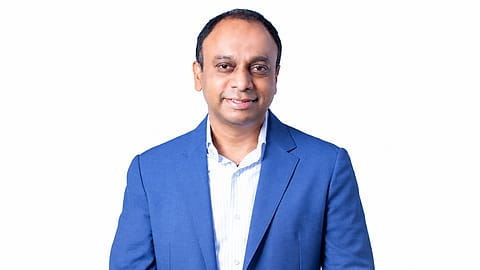
Avi Avula, president of Applied Materials India
Applied Materials is looking to move its India operations further up the semiconductor equipment value chain, with the US company working towards giving its India teams ownership of product lines that can be developed and deployed for its global customers.
“We have become really indispensable for the company, because almost every function, we have a team here supporting it,” Avi Avula, president of Applied Materials India, said in an interview with Fortune India. “Where we are taking this now is can we take ownership for certain product lines from here to end to end.”
The shift builds on an India operation that has already expanded significantly. Applied Materials now has more than 7,000 employees in India, with its workforce growing more than fourfold over the past decade. Employees in India have received more than 750 US patents over the last 10 years, according to company data.
The company has also been building local semiconductor engineering capabilities. In 2024, it established India’s first 300mm R&D lab, with a second phase of expansion currently underway. It is now proposing a 140-acre Advanced Semiconductor Research Park in Bengaluru that would bring cleanroom capabilities, equipment engineering and collaborative R&D with customers and suppliers together at one site.
Avula said the objective is for India’s role to evolve from supporting functions for Applied’s global operations to taking responsibility for specific products.
“So that the headquarters can say, okay, fine, we can trust our India team to take it all. We don’t need to wait for our direction,” he said.
Building a deeper supplier base
The other major piece of the strategy is the development of a local supply chain around semiconductor equipment.
Applied currently works with around 50 production and R&D suppliers in India. Company data shows that these suppliers drove an eightfold year-on-year increase in spending to Applied’s global factories in 2026. The company wants to increase its India-based supply-chain capacity tenfold by 2035 and grow to more than 100 production and R&D suppliers.
Avula said this is more important than simply assembling complete machines in India. “If I’m at this point going to import all my components and subsystems from around the world and then assemble it here and then ship it to Taiwan or Korea, what value am I adding?” he said.
The plan is therefore to develop capabilities progressively, from components to complex modules, subsystems and full systems, and connect products built in India to Applied’s global factories and customers.
Talent is the next constraint
Applied Materials is also expanding the talent pipeline around the semiconductor industry. The company has more than 50 university partnerships and has sponsored more than 150 R&D projects at universities including the IITs and IISc.
{{#most-powerful-women-snapshot-individual.slug}} {{/most-powerful-women-snapshot-individual.slug}} {{^most-powerful-women-snapshot-individual.slug}} {{/most-powerful-women-snapshot-individual.slug}} {{#showRanking}} {{current-rank}} {{/showRanking}} {{#photo.0.url}}
{{name}}
Avula said the challenge is less about the availability of young engineering talent and more about giving graduates the infrastructure and experience needed to work on advanced semiconductor technologies. “The young talent coming out of the universities are the best in the world. But they need a place to work to learn hands on,” he said.
Applied plans to more than double its India R&D workforce by 2035 and expand university partnerships, advanced learning and industry-skilling programmes. Its training initiatives include the Applied Certified Engineer programme and the Applied Certified Technician programme.
The company sees AI as another reason to accelerate this capability. Its India Vision 2035 identifies generative, agentic and physical AI as driving demand for different chip architectures, while rising complexity in logic, memory and advanced packaging is increasing the need for materials and equipment innovation.
For Avula, India has a limited window to establish itself in the semiconductor ecosystem. “Many countries took decades to build this industry. In my view, we have 10 years,” he said.
Follow Fortune India
NEXT STORY