
Intel, 3DGS eye $3.3-billion Odisha bet to build India’s first advanced semiconductor substrate facility
ADVERTISEMENT
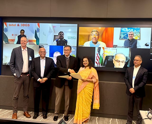
Intel Corporation and Arizona-based 3D Glass Solutions (3DGS) are exploring a $3.3-billion investment in Odisha to set up India’s first advanced semiconductor glass core packaging substrate manufacturing facility, in a move that could significantly deepen the country’s semiconductor manufacturing capabilities.
The proposed project, announced through a memorandum of understanding (MoU) signed with the Odisha government, will focus on advanced glass-based substrates and high-density interconnect packaging technologies used in artificial intelligence (AI), high-performance computing, telecommunications and next-generation electronics.
The facility, proposed to come up in the Bhubaneswar-Khurda region, will include cleanrooms, fabrication units, testing infrastructure and R&D facilities. Intel will act as the technology partner, providing process expertise, technology licensing, quality systems and workforce capability development.
If implemented, the project would mark one of the largest technology investments in eastern India and place Odisha among the emerging semiconductor manufacturing destinations in the country alongside Gujarat, Karnataka and Tamil Nadu.
Odisha seeks semiconductor ecosystem play
The state government said the investment aligns with Odisha Vision 2036, under which the state aims to become a $500-billion economy by 2036 and a $1.5-trillion economy by 2047.
Beyond the direct investment, the project is expected to catalyse a broader semiconductor ecosystem spanning specialty chemicals, advanced materials, glass substrates, electronics manufacturing and export-oriented industries.
According to the investment note, the facility could create around 1,800 direct high-skilled jobs, besides substantial indirect employment through ancillary industries and supply chains.
The proposed unit also aims to position Odisha as a hub for advanced packaging technologies—a segment increasingly becoming central to the global semiconductor industry as chipmakers seek alternatives to traditional transistor scaling.
Push comes amid India’s semiconductor ambitions
The announcement comes as India accelerates efforts to build domestic semiconductor capabilities under the India Semiconductor Mission amid geopolitical shifts in global electronics supply chains.
Global semiconductor companies are increasingly investing in advanced packaging technologies to improve chip performance, energy efficiency and integration for AI-led workloads and data centre applications.
3DGS CEO Babu Mandava said the initiative has the potential to establish India as a global hub for advanced glass substrates and semiconductor packaging. Intel Foundry executive vice-president Naga Chandrasekaran said the collaboration could help accelerate the commercialisation of next-generation packaging solutions globally.
Odisha chief minister Mohan Charan Majhi termed the initiative a “transformational, generational opportunity” that could place the state at the forefront of semiconductor manufacturing, AI infrastructure and digital technologies.
The proposed investment remains subject to regulatory approvals, funding support from the Centre and the state government, and other business conditions.