The FAQs are AI-generated, and Fortune India is not responsible for its content or any associated copyright issues.
India advances in chip value chain with 3DGS facility; semiconductor market expected to hit $103 billion by 2030
/ 2 min read
IESA flags advanced packaging push as a turning point in India’s shift from design strength to manufacturing depth
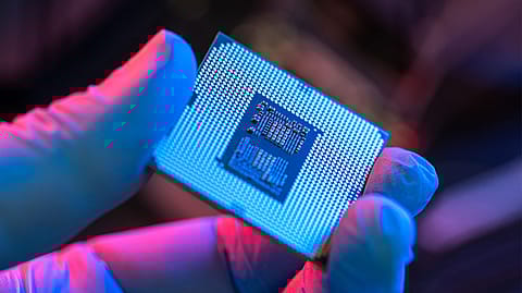
Representational Image | Credits: Getty Images
The inauguration of 3DGS Semicon’s advanced packaging facility in Odisha marks a significant step in India’s semiconductor journey, with the India Electronics and Semiconductor Association (IESA) calling it a clear sign of movement from policy intent to execution.
3DGS Semicon is the India arm of US-based 3D Glass Solutions, known for its glass-based packaging technologies used in high-frequency and high-performance semiconductor applications. The Odisha unit is among the early facilities in India focused on heterogeneous integration—an advanced packaging approach that integrates multiple chips into a single system to improve performance and efficiency.
The facility, inaugurated in the presence of Union Minister Ashwini Vaishnaw and Odisha Chief Minister Mohan Charan Majhi, will manufacture specialised packaging solutions that sit between chip fabrication and final product assembly—an area where India has had limited domestic capacity.
Advanced packaging emerges as key lever
IESA President Ashok Chandak said the unit represents a meaningful capability addition in advanced packaging, increasingly seen as critical to semiconductor performance and system integration.
He noted such investments can help India move beyond participation to value capture by strengthening supply chains, enabling chiplet-led innovation, and supporting next-generation product integration.
With global players looking beyond traditional node scaling, advanced packaging has become a focal point for enhancing performance and efficiency, making domestic capabilities in this segment particularly relevant.
From design base to manufacturing depth
According to Chandak, the development reflects the growing maturity of India’s semiconductor ecosystem, historically anchored in design and engineering.
The addition of packaging and product commercialisation capabilities signals a gradual broadening of the value chain within the country, pointing to progress toward manufacturing more sophisticated semiconductor products.
He added that recent project announcements and groundbreakings indicate stronger execution momentum, supported by coordinated efforts from the Ministry of Electronics and Information Technology (MeitY), the India Semiconductor Mission (ISM), and state governments.
Odisha gains traction as semiconductor destination
With more projects expected this year, the development is seen as reinforcing investor confidence in India’s semiconductor plans.
India is targeting a $400 billion electronics market and a $103 billion semiconductor market by 2030, with such investments viewed as critical to building end-to-end capabilities.
RANK
COMPANY NAME
REVENUE
(INR CR)
(INR CR)
{{#current-rank}} {{current-rank}} {{/current-rank}} {{^current-rank}} {{rank}} {{/current-rank}} {{name}} {{#revenue}} {{revenue}} {{/revenue}} {{^revenue}} {{noi}} {{/revenue}}
The emergence of Odisha as a semiconductor destination aligns with the ‘Make in India’ push, strengthening India’s position in the global semiconductor landscape.
Frequently Asked Questions
NEXT STORY