The FAQs are AI-generated, and Fortune India is not responsible for its content or any associated copyright issues.
India’s maiden 3D chip packaging unit gets ₹1,943 crore push in Odisha; 70,000 panels, 50 million units output planned
/ 2 min read
India’s maiden 3D chip packaging unit gets ₹1,943 Cr push in Odisha; 70,000 panels, 50 million units output planned
The project entails a total investment of ₹1,943.53 crore, including ₹799 crore in central fiscal support and around ₹399.5 crore from the Odisha government. | Credits: Ministry of Electronics and IT
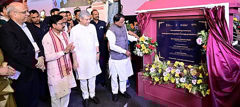
In a significant step towards building a domestic semiconductor ecosystem, the Ministry of Electronics and IT on Saturday oversaw the groundbreaking of India’s first advanced 3D semiconductor packaging facility in Bhubaneswar, Odisha. The ₹1,943.53 crore project—backed by central and state incentives—marks a critical move to localise high-end chip manufacturing capabilities and reduce import dependence in strategic sectors.
The greenfield unit, being set up by US-based 3D Glass Solutions through its Indian arm Heterogeneous Integration Packaging Solutions Pvt Ltd (HIPSPL), will focus on advanced heterogeneous integration and embedded glass substrate technologies. The facility is expected to cater to high-growth sectors including artificial intelligence (AI), high-performance computing, telecommunications, defence electronics, and aerospace.
Investment scale and production roadmap
The project entails a total investment of ₹1,943.53 crore, including ₹799 crore in central fiscal support and around ₹399.5 crore from the Odisha government. Once operational, the unit is designed to produce 70,000 glass panels annually, alongside 50 million assembled semiconductor units and about 13,000 advanced 3D heterogeneous integration (3DHI) modules.
Commercial production is targeted to begin by August 2028, with full-scale capacity utilisation expected by August 2030. The facility will function as a vertically integrated ATMP (Assembly, Testing, Marking and Packaging) unit, a key missing link in India’s semiconductor value chain.
Odisha’s semiconductor ambitions gather pace
With this project, Odisha becomes the only state to host both a compound semiconductor fabrication unit and a 3D glass substrate packaging facility. Officials said the development strengthens the state’s positioning as an emerging hub for electronics manufacturing and advanced chip technologies.
Union Minister Ashwini Vaishnaw noted that India’s electronics production has grown six-fold over the past 12 years, with the country emerging as the world’s second-largest mobile phone manufacturer and a leading exporter in 2025. He added that two semiconductor projects have already been approved for Odisha under the India Semiconductor Mission, with three more proposals under evaluation.
Ecosystem impact and employment potential
The facility is expected to generate significant employment opportunities across engineering, diploma and vocational segments, while catalysing ancillary industries. Industry linkages with global technology players and upcoming policy support—such as Odisha’s IT, AI and Semiconductor Policy 2025—are likely to further accelerate investments.
Beyond semiconductors, the government highlighted parallel infrastructure expansion, including railway projects worth over ₹90,000 crore and enhanced logistics connectivity, aimed at supporting industrial growth in the region.
Frequently Asked Questions
NEXT STORY