
Semicon India 2026: S. Krishnan flags advanced packaging, R&D and manufacturing skills as key priorities
ADVERTISEMENT
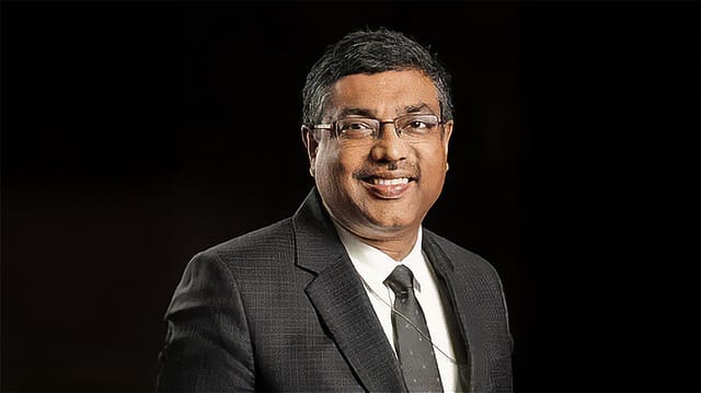
India is shifting its semiconductor focus from establishing manufacturing capacity to building the wider ecosystem needed to support the industry, with advanced packaging, research and development (R&D), and manufacturing talent emerging as key priorities, S. Krishnan, Secretary, Ministry of Electronics and Information Technology (MeitY), said at Semicon India 2026 on Thursday.
Krishnan explained that India had now demonstrated that it was possible to undertake advanced semiconductor manufacturing in the country. “We have demonstrated that it is possible to carry out advanced manufacturing of this nature in the country,” he said.
The next phase, he added, would focus on the ecosystem around semiconductor manufacturing. “The direction in which we are moving and the key of this year’s Semicon conference is to focus on the ecosystem,” Krishnan said.
Semicon 2.0 has six pillars covering areas including semiconductor design, materials, chemicals, gases, equipment, fabs and advanced packaging.
Advanced packaging and R&D emerge as key semiconductor priorities
Krishnan said advanced packaging would be particularly important as the semiconductor industry approaches the limits of traditional methods of increasing computing power.
“All of you are well aware, this is a well-informed audience, you are aware that in some ways we are reaching the limits of Moore’s law and further compute power is going to be possibly built on the basis of better packaging of chips,” he said. “Advanced packaging is the other area which we are conscious of,” Krishnan added.
He also stressed the need to invest in semiconductor R&D as India moves into the next stage of its semiconductor push. “In addition to these four pillars which have significance in a broader sense, we also need to invest in the future in terms of organically pushing this industry in the direction which it needs to go in terms of having research and development,” Krishnan said.
He pointed to international examples where industry, academia and researchers have worked together to advance semiconductor technology. Krishnan cited IMEC in Belgium, efforts in Singapore and Taiwan, and collaborations involving IBM and universities in the US. “Industrial academia and researchers have come together to truly advance the field of R&D, advance the science and the technology relating to semiconductors,” he said. “Clearly that is the direction in which we hope to push in the days to come,” Krishnan added.
He said R&D would receive specific attention under the government’s next phase of the semiconductor programme. “R&D gets a special mention and we are looking to establish this R&D in association with industry so that it serves what exactly industry does,” he said. The government is also looking to address a gap between India’s strengths in chip design and its capabilities in semiconductor manufacturing.
India has chip-design talent but needs advanced manufacturing workforce
Krishnan said human resources would be another important part of India’s semiconductor strategy. He explained that India already has a significant share of the world’s semiconductor design talent but needs to develop a workforce trained for advanced manufacturing. “What we have today is of course 20% of the design, semiconductor design workforce in the world,” he said. “What we don’t have is a workforce which is trained in advanced manufacturing,” Krishnan added.
He said the government would need to work with industry to determine the skills required by semiconductor manufacturers and establish the facilities needed to train workers. “That is a space again where we need to work with industry to figure out the kind of skills that are needed, set up the kind of facilities in association with industry to make sure that we are in a position to support what the industry needs in that area and build those facilities out,” he said.
Krishnan’s comments come as the government moves faster into the second phase of its semiconductor programme. He explained that Semicon 1.0 was originally intended to remain open for about six years. However, the number of applications received and the funding commitments required meant that the government was able to commit the entire resources of Semicon 1.0 within three years of the scheme opening. “We had been in a position to commit the entire resources of Semicon 1.0 within a period of three years of the opening of the scheme and we have had to move necessarily to the next phase of the programme which is Semicon 2.0,” Krishnan said.
He also highlighted the progress under Semicon 1.0, saying five of the 12 approved programmes are now being brought into commercial production. Along with Tata Electronics’ test and pilot production unit, which he said is exporting from its site at Yamaguchi, there are now six locations where semiconductor chip production of various kinds is taking place in India.
Krishnan said detailed guidelines for three of the six Semicon 2.0 pillars had been released. These include machines and materials, setting up additional fabs, and strengthening ATMP and OSAT facilities. He also pointed to faster government approvals as India attempts to accelerate semiconductor investments. Krishnan said Tata Electronics’ application was cleared in less than 100 days. “The CEO of Tata Electronics pointed out that from the date of application to the date of clearance of that application took just 100 days, less than 100 days,” he said.
“That is the speed at which we can work when we have applications which are well prepared looking at all the issues,” Krishnan added.
The broader objective, he explained, is to build an entire semiconductor and electronics ecosystem in India. The government is working to build capabilities ranging from semiconductor design and manufacturing to electronic components, sub-assemblies and modules.
Krishnan said the aim is to combine India’s existing software and design strengths with advanced manufacturing capabilities. “The government of India is attempting to do, what the ministry is attempting to do and what ISM is attempting to do is to truly build out the entire ecosystem in the country,” he said.
He added that India wants to use these capabilities to serve both domestic demand and global markets. “Use India to manufacture for the world, use India to manufacture for India,” Krishnan said.